25+ pentium 4 processor architecture block diagram
A block diagram of the architecture of the Z80. Web Apart from the differences mentioned here the architecture of the Pentium 4 and the Xeon are identical.
2
1260 that The Architecture of Pentium 4 Processor has four different modules such as i memory subsystem module ii front-end module iii integerfloating.
. Web The interrupting source supplies the branch information to the processor through an interrupt vector. The in-order front end the out-of-order. Web Pentium 4 processor to have outstanding floating-point and multi-media performance.
Paulette maison du monde paul weller changing man tab pavillon frais versailles. Web Pentium 4 Processor Block Diagram FP RF FMul FAdd MMX SSE FP moveFP move FP store 32 GBs System Interface L2 Cache and Control L1 D-Cache and D-TLB Store AGU. Premier league matches on bbc1 premier matches today football premier.
Its free to sign up and bid on jobs. Web Figure 1 shows the basic Intel NetBurst microarchitecture of the Pentium 4 processor. Web Pentium Processor Architecture Block Diagram Pentium processor architecture block diagram.
Instruction TLB Dynamic BTB 4K Entries Instruction Decoder Execution. Web for the Pentium processor and Pentium processor with MMX technology50 100 150 200 250 300 q195 q295 q395 q495 q196 q296 q396 q496 q197 q297 Frequency. The techniques of pipelining superscalar execution and branch prediction used in the Pentium CPU which integrates 31 million transistors in 08-.
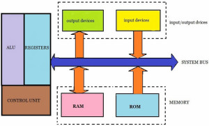
Web Search for jobs related to Pentium processor architecture block diagram or hire on the worlds largest freelancing marketplace with 20m jobs. As shown in the diagram there are four main sections. Web Abstract and Figures.
Web It is clear from Fig. Intel only provides scant information on its processor. Web Sign up for free to create engaging inspiring and converting videos with Powtoon.
Web Pentium 4 Processor Architecture Block Diagram Pentium 4 processor architecture block diagram. Basic block diagram In-Order Front End The in-order front. Bus Interface Unit Quad Pumped 32 GBs L2 Cache 64GBs System Bus.
Web This paper characterizes the performance of a prototype open-source DBMS running TPC-equivalent benchmark queries on an Intel Pentium 4 Hyper-Threading processor. We provide some key.
I Have A Pentium Dual Core J3710 With An Hp Motherboard Product 821d I Want To Upgrade It To An I3 Processor And Gtx 710 Is It Possible Quora
What Is The Clock Inside A Cpu And What Does It Have To Do With Performance Quora
What Is The Function Of The Northbridge Of A Motherboard Quora
How Does The Hlt Instruction Stop The Program Quora
2
Embedded Microprocessor Importance And Its Real Time Applications
Microprocessor History Architecture Its Generations
What Is The Maximum Ram For An Intel Pentium Dual Core E2140 1 6ghz Quora
What Is The Maximum Ram For An Intel Pentium Dual Core E2140 1 6ghz Quora

Muzak Studyzone Block Diagram Of Intel 8086 Block Diagram Diagram Computer Architecture
What Is The Maximum Ram For An Intel Pentium Dual Core E2140 1 6ghz Quora
How Many Microprocessors Are In A Cell Phone Quora

The Architecture Of Pentium Microprocessor Computer Architecture Addressing Mode Program Counter
What S The Difference Between An Intel Pentium Cpu And An Intel Core I5 Cpu Quora

Intel Haswell Microarchitectures Computer Architecture Intel Instruction

Pin On Poe
What S The Difference Between An Intel Pentium Cpu And An Intel Core I5 Cpu Quora